- Your cart is empty
- Continue Shopping
MAX232
MAX232:
- Input supply voltage range, VCC(see Note 1): −0.3 V to 6 V
- Positive output supply voltage range, VS+VCC: − 0.3 V to 15 V
- Negative output supply voltage range, VS−: −0.3 V to −15 V
- Input voltage range, VI : Driver: −0.3 V toVCC+ 0.3 V
- Receiver: 30 V
- Output voltage range, VO: T1OUT, T2OUT : VS− − 0.3 V to VS+ + 0.3 V
R1OUT, R2OUT: −0.3 V to VCC+ 0.3 V
Product Description
DESCRIPTION:
-
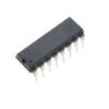
The MAX232 is a dual driver/receiver that includes a capacitive voltage generator to supply TIA/EIA-232-F voltage levels from a single 5-V supply. Each receiver converts TIA/EIA-232-F inputs to 5-V TTL/CMOS levels.
-
These receivers have a typical threshold of 1.3 V, a typical hysteresis of 0.5 V, and can accept ±30-V inputs. Each driver converts TTL/CMOS input levels into TIA/EIA-232-F levels. The driver, receiver, and voltage-generator functions are available as cells in the Texas Instruments LinASIC library.
- Technical sheet: https://pdf1.alldatasheet.com/datasheet-pdf/view/27251/TI/MAX232.html
FEATURES:
-
Meets or Exceeds TIA/EIA-232-F and ITU Recommendation V.28
-
Operates From a Single 5-V Power Supply With 1.0- mF Charge-Pump Capacitors
-
Operates Up To 120 kbit/s
-
Two Drivers and Two Receivers ±30-V Input Levels
-
Low Supply Current 8 mA Typical
-
ESD Protection Exceeds JESD 22− 2000-V Human-Body Model (A114-A)
-
Upgrade With Improved ESD (15-kV HBM) and 0.1-mF Charge-Pump Capacitors is Available With the MAX202
Applications:
− TIA/EIA-232-F, Battery-Powered Systems, Terminals, Modems, and Computers


Reviews
There are no reviews yet.